
Italian-Russian center for intelligent material applications
Русский-
News
- 10.03.2022
NTEGRA Spectra Nanolaboratory
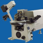 Type: Nanolaboratory
Fabricator: NT-MDT (http://www.ntmdt.ru/)
Capabilities:
Studying objects’ optical properties beyond the diffraction limits by means of Scanning Near-field Optical Microscopy and the effect of local tip enhanced Raman scattering (TERS). The capability of mapping the optical properties distribution (light transmission, light scattering, light polarization, etc.) as well as carrying out Raman scattering spectroscopy with flat XY resolution up to 50 nm.
The system is capable of working in the mode of registration of spatial 3D distribution of luminescence spectrum and Raman light scattering, as well as various scanning probe microscopy modes that include nanoindentation, nanomanipulation and nanolithography.
Along with the optical observation, NTEGRA Spectra allows investigating the object with a set of SPM methods: AFM, MFM, STM, Scanning Near-field Optical Microscopy, Force spectroscopy.
Implemented methodics:
Roman microscopy
At the moment the equipment is being used for studying silicon nanocrystals in dielectric matrix, as well as thin films of amorphous and of crystal silicon with thickness 5 nm.
Lazer excitation with the wave length, nm:
473, 632.8, 785
Measurement range and interval for Roman shifts, sm-1
190-800, 0,7
190-8500, 9
XY method locality, nm: ~ 200
XY maximum scanning range, um: ~ 50
Z scanning range, um: 76
Scanning Near-field Microscopy
Modes:
Transverse force microscopy / Luminiscent reflection transmission method
Lazer excitation with the wave length, nm: 473, 532, 632.8
Maximum scanning range:
XY sample scanning, um: ~ 50
XY probe scanning, um: ~ 100
Fiber aperture, nm: < 100
Atomic force microscopy
Maximum scanning range:
XY sample scanning, um: ~ 1, 50, 100
XY probe scanning, um: ~ 100